From Stopping Tumor Movement to Long-lasting Folding Electronics
by Alan S. Brown
Research highlights from Kavli Nanoscience Institutes

The Author
This collection features a mix of biological and physical nanoscience insights. At the top, we discuss how Kavli researchers isolated the mechanism that enables brain cells to move and grow—and their research partners used this insight to keep cancer masses from moving. Also on the bio side, we discuss a new camera fast enough to let us visualize how nerve signals move through cells. In terms of electronics, we discuss how researchers have found some real-world uses for graphene grown at room temperature, including one that multiples the lifespan of folding electronics by a factor of 10. We also look at color centers as a possible route to quantum devices and the power of a good, deep clean to unlock aluminum nitride’s potential for generating ultraviolet light.
Stopping cancer from hijacking brain formation mechanism
When it comes to our bodies, our brains are the final frontier. They are not only difficult to access but their billions of neurons and trillions of connections make them extremely complex. At the Kavli Institute for NanoScience Discovery at Oxford, Elena Seiradake has teased out how two different proteins work together to direct embryonic neurons in growing brains to the right place. Using a technique called X-ray protein crystallography, she found that the sugars on the surfaces of proteins Unc5 and GPC3 determine how they interact with one another. By introducing a change to these proteins, Seiradake was able to disrupt brain development. Based on these insights, her collaborators at the Universities of Barcelona and Lyon realized that cancers use the same proteins to spread. By changing the proteins in neuroblastoma cancer cells, they prevented the tumor from moving as a tightly packed mass of cells.
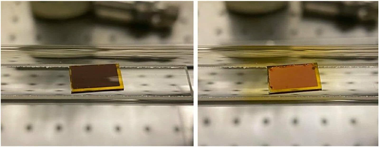
Graphene: ready for large-scale use?
Graphene could vastly improve the durability of bendable electronics, smart health patches, and folding display screens, according to research undertaken by Nai-Chang Yeh, a board member of the Kavli Nanoscience Institute at Caltech. In 2015, Yeh showcased a room-temperature route to making one-atom-thick sheets of graphene in 15 minutes. This was a break from most conventional methods, which relied on high temperatures (more than 1000° C) and hours of processing. Her latest research makes the case for graphene in several applications. One paper showed that growing graphene on flat copper wires in electronics allowed her to fold them 200,000 times without damage, 10 times longer than untreated copper. Second, graphene can protect flexible circuits created by inkjet printers. Finally, coating gold-plated body sensors with graphene slows down the rate at which sweat corrodes the gold. Yeh’s graphene production method uses a methane- and hydrogen-based plasma-enhanced chemical vapor deposition process that cleans and polishes the target surface and deposits high-quality graphene films.
Filming nerve signals on the move
Nerve signals course through the body at speeds of 100 to nearly 300 miles per hour. Visualizing these bursts would go a long way towards understanding the workings of our brains, eyes, and even our fingertips. Now, thanks to a high-speed camera created by Lihong Wang, an affiliate of the Kavli Nanoscience Institute at Caltech, there is a way to do it. Wang is a master of high-speed cameras. In fact, his compressed ultrafast photography (CUP) camera is fast enough to track a laser pulse as it ricochets inside a small cavity. To visualize nerve signals, Wang added an interferometer to CUP. This allows the camera, called Diff-CUP, to split its light into two sister beams, pass one through an object, and then recombine them into a single beam. Because the beam that went through the object is now out of synch with its sister, merging them creates interference that can be mined mathematically for information. The result are amazing pictures of nerve pulses moving through the body. Diff-CUP can also image electromagnetic pulses moving through a semiconductor, lithium niobate.
Color your quantum
Color centers, which can arise at “defect” sites in wide-bandgap materials such as diamond, have long been considered candidates for quantum devices. Hexagonal boron nitride (hBN) hosts color centers that are particularly bright, stable at high temerparures, and have optically addressable spin properties, all features that are highly desireable. However, until now use of hBN color centers has been limited by their inherent randomness. Researchers Shaul Aloni, Alex Zettl, a member of the Kavli Energy NanoScience Institute at UC Berkeley, and Cong Su, a postdoc in Zettl’s group, overcome this barrier by twisting two layers of hexagonal boron nitride at an angle to one another. This allowed them to tune the brightness of the color centers (and turn them off completely) using an electrical current. An electron beam treatment lets them control the position of the centers. The team plans further characterization to see if they can use the material to build quantum systems.
Cleaning unlocks aluminum nitride’s power
Aluminum nitride (AlN) is an unusual semiconductor because it combines excellent electrical insulation properties with high thermal conductivity. It can be used, for example, to whisk away heat in high-powered lasers and hot electronics. Researchers also think they could create high-powered ultraviolet lasers and LEDs by growing a variation of the material, nitrogen-polar aluminum nitride, on AlN’s surface. They do this by a process called molecular beam epitaxy (MBE), which grows perfect crystals. When they use this on AlN, however, all they can do is create small islands of the polar material due to native surface aluminum oxide. A team led by Debdeep Jena and Huili Grace Xing, senior researchers at the Kavli Institute at Cornell for Nanoscale Science, have found a way to remove the oxide that is compatible with MBE and has yielded high quality epitaxial nitrogen-polar aluminum nitride films. Their technique adds aluminum to react with aluminum oxide on the semiconductor’s surface, creating a volatile form that evaporates away.