Layer by Layer: The Ascent of Nanoscale Two-Dimensional Materials
by Ivan Amato
The emerging ability to precisely engineer 2D materials could open design pathways to future-generation microelectronic devices, improved batteries, and even new types of liquid crystals.

The Author
The Researchers
TO UNDERSTAND TWO-DIMENSIONAL MATERIALS, it might help to think of a sandwich.
Nanoscience is all about understanding and manipulating the world on atomic and molecular scales, and one way scientists are doing this is with sheets of materials that, incredibly, are no more than a single or a few atoms thick. Why do this? Because by stacking these “2 dimensional” sheets like meats in a deli sandwich – a metaphor that Paul Weiss, the Fred Kavli Chair in NanoSystems Science at the University of California, Los Angeles, recently floated at a symposium celebrating Kavli-sponsored research – scientists are finding that they can engineer brand new 2D materials capable of manipulating electrons, photons, crystal vibrations and other signals with more finesse than ever. From this control, they say, will come technology.
Nanoscientists already are synthesizing and studying an ever-diversifying variety of 2D materials with optical, metallic, semiconducting, electrically insulating and many other tunable properties. To understand where they’re going, three nanoscientists at the forefront of this emerging field recently spoke with The Kavli Foundation about how 2D materials are opening pathways to new ways of asking and answering questions about what underlies the behavior of materials. This, in turn, may bring about new materials that can lead to new generations of existing high-tech technologies, and even to technologies the world has never seen before.
- TONY HEINZ, Ph.D. - holds joint appointments in the Departments of Physics and Electrical Engineering at Columbia University and is the North American Regional Editor of the new Institute of Physics journal titled 2D Materials.
- DAVID MULLER, Ph.D. - is Professor of Applied and Engineering Physics at Cornell University and co-director of the Kavli Institute at Cornell for Nanoscale Science.
- JOSHUA GOLDBERGER, Ph.D. - is Assistant Professor of Chemistry at the Ohio State University in Columbus.
The following is an edited transcript of a roundtable discussion. The participants have been provided the opportunity to amend or edit their remarks.
THE KAVLI FOUNDATION: Materials scientists can combine the atoms of the Periodic Table into an infinitude of specific compositions and they can arrange those compositions into another infinitude of structures. A primary conceit of nanoscience is that the nanoscale is special, that understanding and controlling matter on this scale is particularly empowering both in scientific and technological pursuits. What is it about 2D materials, just one among many subfields of nanoscience, that makes it stand out for you and others who are moving this field forward?
DAVID MULLER: When we think of atoms, we think of them as the smallest building units for materials that you can get. But you need to build stuff with them. I think of 2D materials as stuff that has been thinned down so that you can’t make it any thinner. These materials are one atom or one molecular layer thick. And so they amount to a new kind of basic building block for entirely new categories of materials.
TONY HEINZ: To add a little historical comment, there has been much interest and research in quasi-2D materials over the years. In particular, in layered manmade structures, like semiconductor quantum wells, we can constrain electrons to one quantum state in the perpendicular direction, but allow free movement along the plane of the layers. These systems have revealed fascinating and useful electronic and optical properties. We are building on that foundation, but now with different synthetic methods and characterization tools to explore the new regime of atomically thin 2D materials.

JOSHUA GOLDBERGER: One aspect of 2D materials that I find fascinating is that while they have atomic-sized thicknesses, they are robust enough to allow researchers to learn how to manipulate the properties of materials at the atomic size-regime. In [Richard] Feynman’s famous lecture about nanoscience, “There’s plenty of room at the bottom,” he eloquently argued for learning how to manipulate and control the properties of materials that have dimensions less than hundreds of atoms. However, making materials in which one dimension is less than two nanometers, or ten atoms thick, becomes incredibly challenging in part because very often at this size scale, materials are chemically and mechanically unstable and incredibly reactive in air. In contrast, the intrinsic 2D bonding nature of atoms in these materials makes them strong enough to handle and manipulate.
“One aspect of 2D materials that I find fascinating is that while they have atomic-sized thicknesses, they are robust enough to allow researchers to learn how to manipulate the properties of materials at the atomic size-regime.” —Joshua Goldberger
Indeed, many materials that we have been studying for a long time are intrinsically 2D and even can be found in nature. Graphite, for one, is the most stable allotrope of carbon. It consists of a 2D honeycomb network of covalently linked carbon atoms within each layer, but these layers are held together by weak van der Waals forces. That is why they slide off from pencil “leads” and can leave marks on papers, and can be exfoliated to prepare single atom thick layers of “graphene.” It is the same with molybdenum disulfide (MoS2), an important industrial lubricant and a famous example of a large family of van der Waals solids called layered metal chalcogenides. While the interlayer interaction in these materials is quite weak, there exists an appreciable amount of electronic communication between neighboring layers. This gives researchers the power to tune the electronic and optical properties of these layers by peeling them apart and restacking them with other layers.
TKF: Could each of you describe the research landscape in the area of 2D materials, or at least part of that landscape that you know well or find particularly interesting

GOLDBERGER: The research landscape of 2D materials ranges from the synthesis of new materials, to understanding the properties that emerge at the single layer scale and restacking these layers to form new properties, to exploiting these properties in both existing and emerging technologies. Coming from the discipline of chemistry, one aspect that I particularly find fascinating is the creation of unique 2D materials that don’t occur in nature and whose properties can be changed using chemical methods. Just as carbon can form into various low-dimensional allotropes (graphene sheets, carbon nanotubes, C60 and other fullerenes) that feature fundamentally different and technologically useful electronic and optical properties compared to graphite, my group tries to create single low-dimensional derivatives of other very common 3D crystal structures. Doing so can similarly give these materials properties that they wouldn’t normally have, but requires us to think about how to terminate the lattice to keep the natural chemistry satisfied.
"To me, 2D materials represent an exciting frontier of research. One of the fascinating aspects is the ability to create electronic states in combinations of 2D materials that are different than what you get for either material itself." —Tony Heinz
For example, carbon atoms traditionally assemble into two major lattice-types, the diamond lattice type in which every carbon is covalently bonded to four other carbon atoms, and the graphite structure, where every carbon atom is covalently bonded to three other carbon atoms while sharing one pi-bond. However, silicon and germanium, which are the most technologically useful materials of our current age, only crystallize into a diamond-lattice type, since their pi-bonding interactions are much weaker. My group has recently created single atom thick germanium graphane analogues, or germananes, in which the germanium atoms still maintain the same honeycomb network as carbon does in graphene, yet every germanium atom needs a covalent bond to a surface-terminating group, such as hydrogen, or an organic group like methyl (-CH3), to have four bonds. In contrast to the bulk germanium lattice, the emission and absorption of light in these 2D germananes occurs much more readily, making them more useful in optoelectronic applications such as light emitting diodes, lasers and solar cells. Also, because we can readily exchange the surface terminating groups with other chemical groups, this gives us the power to locally tune the properties of the material via covalent chemistry.
This is just one of the fascinating challenges with 2D materials: to learn to what extent we control properties of the layer just by tuning the chemistry above and below the layers. It can open up vast new scientific and technological opportunities in sensing, electronics and optoelectronics.
MULLER: We are attracted to these materials because they constitute new classes of systems that can have novel properties. Understanding what happens when you take materials down to the thinnest thing possible is compelling. We are at the beginning of determining what is possible. Can you restack these sheets to create new systems that do things that no materials have done before? There is a lot of interest in exploiting these for applications, ranging from electronics, solar cells, optoelectronic devices, even for things we haven’t thought of yet. This notion – that as a result of stacking different 2D materials like elements, properties in different places within the stack can be different and influenced by everything around – is exciting.

Although graphene is the most developed 2D material, the community is rapidly developing new classes of 2D materials, as Josh just mentioned. From my perspective, graphene could be considered Chapter One of the story of 2D materials. It is the perfect embodiment of the 2D limit. A long second chapter is, however, now being written about other types of 2D materials. These materials may have very different properties from graphene. Single layers of MoS2, for example, are semiconductors, while graphene is a special type of metal. Also, the spin of electrons in MoS2 can be accessed by light, which is not possible in graphene. Like graphene, however, atomically thin MoS2 is strong, stable, flexible, and highly tunable by the external environment. So the development of a broad class of such new 2D materials has, in my view, great potential for the coming years.
There is, moreover, already a third chapter of the story, which is probably the most far-reaching and important aspect of 2D materials. This is the notion of combining these layers together in distinctive sandwich structures. Since these 2D materials are stable on their own, they can be combined with one another with few constraints. Consequently we can expect the emergence of many new properties and applications. This topic is just at the frontier of current research and will surely lead to new and unanticipated possibilities.
MULLER: To expand on Tony’s third point, the real applications breakthrough will be for 2D materials to do things others materials can’t do at all; we might not want to replace computer chips with graphene. While there has been a lot of progress in electronic materials, mechanical properties of materials have not been developed as much. In 2D materials, mechanical properties are remarkable. You can design them to assemble almost in Origami fashion. Graphene has the stiffness of tissue paper, so you could make it into mechanical objects that fold up to have phenomenal surface area. And such objects could be incredibly sensitive to chemical reactions and have a huge ability to store things on surfaces, perhaps for applications like supercapacitors and batteries. Real strengths and applications will come when we figure out the rules and learn to fit 2D materials together and combine ordered areas with disordered ones because that is so often where interesting properties arise.
“The real applications breakthrough will be for 2D materials to do things others materials can’t do at all.” —David Muller

TKF: Could each of you say something about the questions or materials that you find most compelling at the moment?
HEINZ: Our interest is to understand how electrons behave in these ultrathin materials and how light interacts with these electrons. If you absorb light in a material, you create an electron in an excited state along with a [positively charged] hole where the electron used to be. In atomically thin materials, the resulting electron and hole interact very strongly with one another because they are so close together. We are studying these interactions using a variety of experimental approaches. Although our motivation is more on the fundamental physics side, we need to understand these basic properties in order to develop novel light emitters, detectors and modulators based on 2D materials. We are also exploring what happens when two atomically thin layers are placed in contact with one another. How do electrons jump between the two layers? How does the interaction of light with the two layers in contact with one another differ from that when they are well-separated?
MULLER: 2D silica glass is my favorite new material. We stumbled across this by accident. We were looking at electron microscope images of what we expected to be graphene, but instead saw some strange and pretty patterns. When we zoomed up to see the atoms, we just stared and said to each other, "wow, do you know what that is?” What we had was silica, the same stuff as window glass, but only two silicon atoms thick, and it looked like the 80-year old drawings of how people imagined the atoms in a glass might be arranged. The atoms for the silica had evidently been deposited from the quartz furnace tube, which had been overheated. It formed with two layers and then remained stable; all of the bonds were tied up and it was happy. There are no defects in it, but it is completely disordered just like in the amorphous bulk forms of glass. It also is surprisingly rigid and generally has the same properties as bulk glass. And it is incredibly, incredibly, incredibly stable. With our electron microscope, we can image our 2D glass samples and see every atom. Then we can watch it melt, and start to see new details about its transition from glass to liquid and back to glass again. We can see that glass has no memory of previous states because the specific structure is different with each cycle of melting and solidifying. Even at two molecular layers, glass is an incredibly good insulator. But it’s different from most other 2D materials, such as graphene, in that it behaves much like the corresponding bulk material. Graphene is extremely different from graphite.

HEINZ: To me, 2D materials represent an exciting frontier of research. One of the fascinating aspects is the ability to create electronic states in combinations of 2D materials that are different than what you get for either material itself. In the usual case of materials made of thin layers – but which do not reach down to the atomic scale – composite materials have properties that are essentially the sum of the individual components. This situation changes when the layers are only a few atoms thick. On the nanoscale, as prevails in 2D materials, we can change the properties of electrons simply by bringing materials together or by tuning their thickness. This provides us with intriguing possibilities for the control of electrons. And it is not just a lot of fun. It means that we can manipulate electrons, and thus the control of the flow electrical currents, electron spin, and interactions with light. These are the fundamental ingredients for new types of electronic and photonic devices. The strong coupling of atomically thin 2D materials with the external environment also endows them with unique properties compared with conventional material systems.
MULLER: Another beauty and attraction of 2D materials is that you can make a material that is one atom thick, but as wide and big as a TV screen. We have been able to use tools like molecular beam epitaxy (MBE) and put down one layer of atoms at a time on crystal substrates so that you can do interface physics, but those preparations tend to be on relatively small pieces and not on a large scale, and it takes very expensive equipment. But when you see how simple it is to make graphene, you get some idea of what might be possible with 2D materials. With little more than a furnace and reel-to-reel processing – you grow it on a copper reel and peel it off with a plastic one – the carbon in one Girl Scout cookie could make enough graphene to cover a football field. The idea that I can get this atomic scale precision, without having to rely on precise growth control and expensive equipment, suggests that applications with 2D materials could be large scale, big things. I can imagine the promise of covering football fields, rather than thinking only about small-scale electronic devices. The 2D materials might work because of their nanoscale structure, but we could think in terms of agricultural length scales. And because we are talking about materials that are one atom or a molecular layer thick, you can think about making, for example, large-area solar cells that are light enough to get into space affordably. Or you can think of solar sails in space that could collect sunlight and drive a spaceship.
TKF: Tony, could you comment on the significance on the roll out in June by the Institute of Physics of the journal titled “2D Materials” and for which you are an editor?
HEINZ: The new journal reflects the feeling that a major new subfield of science has arrived – and one that is attracting and will continue to attract great interest worldwide. Another motivation for starting the journal was to provide a forum where researchers with very different disciplinary backgrounds can communicate with one another. 2D materials are being developed and studied by researchers with backgrounds in chemistry, materials science, physics, electrical engineering and other fields. They all provide important knowledge and perspectives to propel the field forward, but often speak somewhat different languages. The emergence of a recognized new subfield – helped along, we hope, by the journal – will serve to link together investigators in these different communities who share common interests in 2D materials. A natural question – and one we considered in starting the journal – is whether the driving force for 2D materials is interesting science or the promise of technology. At the moment, the answer is both. That is what makes the field so exciting. There are not only fascinating basic science issues, but also many new technology directions made possible by the emergence of 2D materials.
Sidebar: From Scotch Tape to Deli Sandwiches: Future 2D Materials

Among the naturally occurring 2D materials is graphite, whose bulk forms are composed of atomically thin sheets of graphene: carbon atoms arranged in chicken-wire sheets, writ nanosmall. Those sheets are shed from pencil “leads” to leave marks on paper, to mention the most familiar application of 2D materials. And it was the Noble-Prize-winning discovery, reported in 2004 by Kostya Novoselov and Andre Geim, that revealed it was possible to successively remove sheets from graphite flakes – using adhesive tape, no less! – all of the way to the logical and physical conclusion: to an atomically-thin graphene sheet.
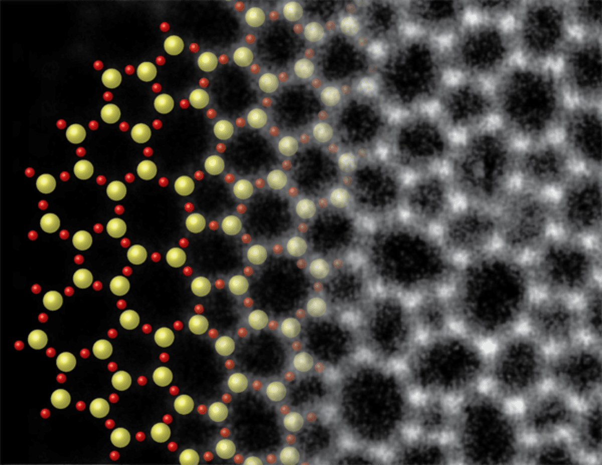
Molybdenum disulfide is a great lubricant because it forms into loose layers that readily slide from one another. Shown here are two views - via optical microscopy on the left (with an overlay of the material’s atomic structure) and via photoluminescence on the right - of a nanoscale MoS2 crystal consisting of two molecular layers with part of one layer broken away. Together, the images reveal the relationship between atomic locations, the number of molecular layers, and the emissive properties of the 2D material. (Credit: Tony Heinz)
Besides the Scotch tape technique to isolate layers of graphene, molybdenum disulfide and other so-called van der Waal solids (a kind of 2D material), researchers have been making other types of 2D materials by deploying vapor or solution phase deposition methods atop substrate surfaces and a dipping procedure. “Nanosheet multilayer assemblies are formed by alternately dipping substrates in colloidal suspensions of charged nano-sheets and in aqueous solutions of polyelectrolytes having the opposite charge,” stated a 22-author review of 2D materials published in the journal ACS Nano. Roundtable participants Joshua Goldberger and Tony Heinz are among the authors.
The emerging ability to precisely engineer the charge environment along the surface area of 2D materials is opening design pathways to, among other things, future-generation microelectronics devices – in arenas with names like spintronics and valleytronics, the latter referring to the energy landscapes of the materials – that do more computing using less energy and even to never-before-seen devices.
Pushing forward into the “deli sandwich” approach of stacking different nanosheets into multilayer films “can lead to improved properties in the areas of supercapacitors, pseudocapacitors, photoconductive materials, and heterojunction photodiodes as new magnetic materials and as magneto-optical components,” according to the ACS Nano review. Additional applications include the following: batteries, magneto-optical materials in which the magnetization is affected by light, photoconductors, high dielectric constant materials, and new types of liquid crystals.