Micron-sized Robots Get Smarter
by Alan S. Brown
Nanoscience has that rare capacity to make what was once old new again

The Author
The Researchers
Nanoscience has that rare capacity to make what was once old new again. Take, for example, Hall-effect sensors, which are often used to find the location of a rotating part like an auto engine’s camshaft. Add nanoscience, and now they can detect small magnetic changes even in a strong magnetic field—and do it down to temperatures where traditional Hall sensors no longer function. Or look at metal-organic frameworks, crystals made of metal hubs attached to organic chemical rods that are mostly air. By added sequences of different metals, it may one day become possible to program them to perform complex chemical reactions. This month, we will clue you in on these breakthroughs and more.
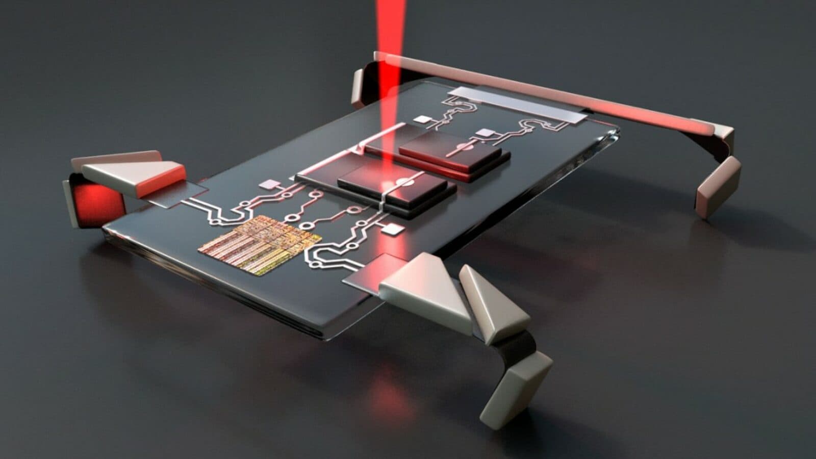
Micron-sized robots get smarter
In 2018, researchers unveiled a microrobot the size of a paramecium and mass-produced more than one million of them on a single 4-inch silicon wafer. Now they have made that robot smarter. The original robot had a built-in photovoltaic cell for power and legs that bent. Yet its actuator system (legs) did not respond to standard electrical control signals. The researchers, Paul McEuen and Itai Cohen of the Kavli Institute at Cornell for Nanoscale Science and their former graduate student (now a professor at University of Pennsylvania), Marc Miskin, have remedied this problem. Their new actuator system responds to conventional electrical signals the way a full-sized servomotor would. This opens the door for smarter and more complex robots in the future, perhaps ones that could restructure a material or suture a blood vessel after an operation.
Sensing small magnetic changes
Imagine trying to listen to a bird sing while a chain saw is running. That is what it is like to detect miniscule changes in magnetic fields when they are near larger magnetic fields. Katja Nowack, a member of the Kavli Institute at Cornell for Nanoscale Science, has developed a tiny sensor that does exactly that. It sandwiches graphene—a material that often crumples and loses its properties when deposited on a semiconductor—between two sheets of hexagonal boron nitride to achieve the feat. Not only does it perform as well as the best Hall sensors at room temperature, but unlike them, works at nearly absolute zero temperature. She hopes to use the sensor to image quantum materials and explore how magnetic fields interfere with some superconductors.
Programmed open crystals
Metal-organic frameworks (MOFs) have become the most studied family of chemicals in the world since Kavli Energy NanoSciences Institute at UC Berkeley researcher Omar Yaghi discovered them 25 years ago. MOFs consist of metal hubs linked with organic rods. This open structure enables other molecules to move through the MOF, which can grab them and perform chemical reactions on them. Researchers used this feature for everything from hydrogen and carbon storage to catalysis and removing drinking water from desert air. The next step is to use a combination of different metals (rather than just one) to program MOFs to do more complex things, like release different drugs into the body at different times or break down active ingredients into harmless substances when they are no longer needed. Now Yaghi’s group, teaming up with Ruhr-Universität Bochum, has found a way to measure the arrangement of metal sequences in a MOF so they can be controlled and reproduced. This is the first step on the road to coding MOF’s to make custom molecules.
Band(gap) tune-up
For an electron or photon to travel, it needs to “jump” out of an atom. The amount of voltage needed to do this is called the bandgap, and it determines a semiconductor’s electrical and optical properties. While scientists have learned to adjust bandgaps by combining two materials, it is a hit-or-miss proposition. That may not be the case for at least one atomically thin alloy, rhenium niobium disulfide. Using electron microscopy and statistical analysis, Berkeley researchers Alex Zettl, a member of the Kavli Energy NanoSciences Institute, and Marvin Cohen discovered meandering stripes of rhenium and niobium running through the crystal. By controlling those stripes—and by adding additional layers of the alloy—they developed a new way to adjust the bandgap. The ability to engineer exactly the bandgap they need could improve the performance of next-generation optoelectronics, thermoelectrics, and sensors.
Applying quantum to emerging technologies
The U.S. Department of Energy will spend $625 million over five years to fund five new U.S. quantum information centers. Part of the National Quantum Initiative, the centers plan to apply quantum technology to everything from scientific computing and fundamental physics and chemistry research to the design of solar cells and pharmaceuticals. Caltech will participate in three of them. Kavli Nanoscience Institute researcher Oskar Painter is among the top researchers participating in Q-NEXT, which seeks to build large networks based on quantum entanglement. These could be used for secure data sharing, distributed computation, and as sensor arrays.