New Thin, Flat Lenses Focus Light as Sharply as Curved Lenses

May 19, 2015
(Originally published by Caltech)

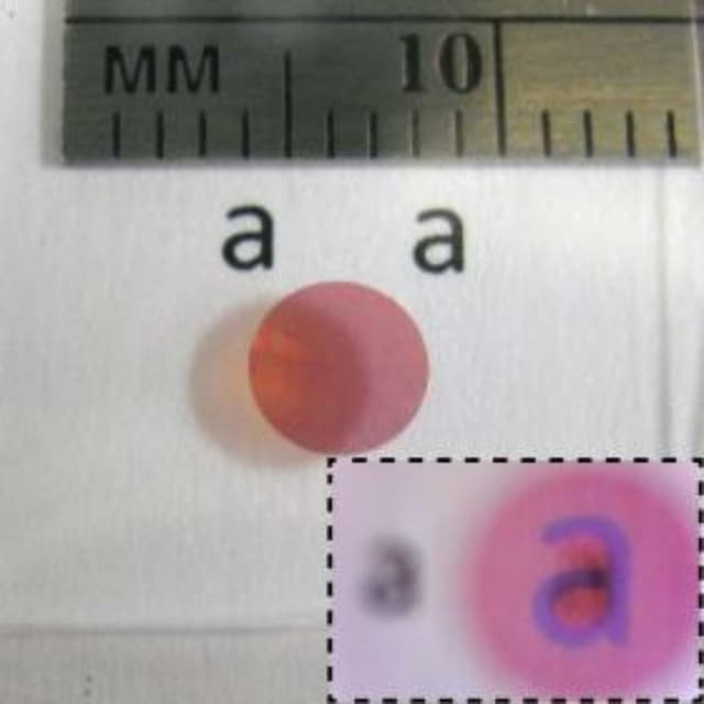
A high contrast transmitarray lens designed for red light (650nm), and magnification by the lens (inset). The lens is made of over 140 million 360nm-tall amorphous silicon nano-posts. (Elsevier/Nature Communications)
Lenses appear in all sorts of everyday objects, from prescription eyeglasses to cell-phone cameras. Typically, lenses rely on a curved shape to bend and focus light. But in the tight spaces inside consumer electronics and fiber-optic systems, these rounded lenses can take up a lot of room. Over the last few years, scientists have started crafting tiny flat lenses that are ideal for such close quarters. To date, however, thin microlenses have failed to transmit and focus light as efficiently as their bigger, curved counterparts.
Caltech engineers have created flat microlenses with performance on a par with conventional, curved lenses. These lenses can be manufactured using industry-standard techniques for making computer chips, setting the stage for their incorporation into electronics such as cameras and microscopes, as well as in novel devices.
"The lenses we use today are bulky," says Amir Arbabi, a senior researcher in the Division of Engineering and Applied Science, and lead author of the paper. "The structure we have chosen for these flat lenses can open up new areas of application that were not available before."
The research, led by Andrei Faraon (BS '04), assistant professor of applied physics and material science, appears in the May 7 issue of Nature Communications.
The new lens type is known as a high-contrast transmitarray. Made of silicon, the lens is just a millionth of a meter thick, or about a hundredth of the diameter of a human hair, and it is studded with silicon "posts" of varying sizes. When imaged under a scanning electron microscope, the lens resembles a forest cleared for timber, with only stumps (the posts) remaining. Depending on their heights and thicknesses, the posts focus different colors, or wavelengths, of light.
A lens focuses light or forms an image by delaying for varying amounts of time the passage of light through different parts of the lens. In curved glass lenses, light takes longer to travel through the thicker parts of the lens than through the thinner parts. On the flat lens, these delays are achieved by the silicon posts, which trap and delay the light for an amount of time that depends on the diameter of the posts. With careful placement of these differently sized posts on the lens, the researchers can guide incident light as it passes through the lens to form a curved wavefront, resulting in a tightly focused spot.
The Caltech researchers found that their flat lenses focus as much as 82 percent of infrared light passing through them. By comparison, previous studies have found that metallic flat lenses have efficiencies of only around a few percent, in part because their materials absorb some incident light.

(a) Schematic of the aperiodic high contrast transmitarray lens used to realize a high-NA micro-lens. (b) Optical microscope image of a fabricated high contrast transmitarray lens lens with large NA. Scale bar, 100 μm. (c,d) Scanning electron microscope images of the silicon posts forming the high contrast transmitarray lens micro-lens. Scale bars, 1 μm. (Elsevier/Nature Communications)
Although curved glass lenses can focus nearly 100 percent of the light that reaches them, they usually require sophisticated designs with nonspherical surfaces that can be difficult to polish. On the other hand, the design of the flat lenses can be modified depending upon the exact application for which the lenses are needed, simply by changing the pattern of the silicon nanoposts. This flexibility makes them attractive for commercial and industrial use, the researchers say. "You get exceptional freedom to design lenses for different functionalities," says Arbabi.
A limitation of flat lenses is that each lens can only focus a narrow set of wavelengths, representing individual colors of the spectrum. These monochromatic lenses could find application in devices such as a night-vision camera, which sees in infrared over a narrow wavelength range. More broadly, they could be used in any optical device involving lasers, as lasers emit only a single color of light.
Multiple monochromatic lenses could be used to deliver multicolor images, much as television and computer displays employ combinations of the colors red, green, and blue to produce a rainbow of hues. Because the microlenses are so small, integrating them in optical systems would take up little space compared to the curved lenses now utilized in cameras or microscopes.
Although the lenses currently are expensive to manufacture, it should be possible to produce thousands at once using photolithography or nanoimprint lithography techniques, the researches say. In these common, high-throughput manufacturing techniques, a stamp presses into a polymer, leaving behind a desired pattern that is then transferred into silicon through dry etching of silicon in a plasma.
"For consumer applications, the current price point of flat lenses is not good, but the performance is," says Faraon. "Depending on how many of lenses you are making, the price can drop down rapidly."
The paper is entitled "Subwavelength-thick lenses with high numerical apertures and large efficiency based on high-contrast transmitarrays." In addition to Arbabi and Faraon, other Caltech coauthors include graduate student Yu Horie, senior Alexander Ball, and Mahmood Bagheri, a microdevices engineer at JPL. The work was supported by the Caltech/JPL President's and Director's Fund and the Defense Advanced Research Projects Agency. Alexander Ball was supported by a Summer Undergraduate Research Fellowship at Caltech. The device nanofabrication was performed in the Kavli Nanoscience Institute at Caltech.