Nanoscale Probe Reveals Interactions Between Surfaces and Single Molecules

(Originally published by the Univeristy of California, Los Angeles)
November 17, 2010
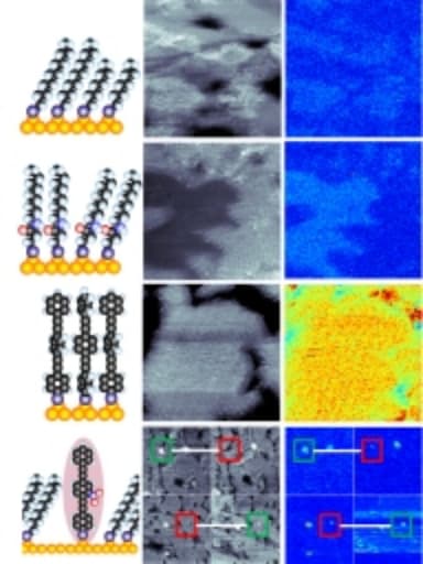
As electronics become smaller and smaller the need to understand nanoscale phenomena becomes greater and greater. Because materials exhibit different properties at the nanoscale than they do at larger scales, new techniques are required to understand and to exploit these new phenomena. A team of researchers led by Paul Weiss, UCLA’s Fred Kavli Chair in NanoSystems Sciences, has developed a tool to study nanoscale interactions. Their device is a dual scanning tunneling and microwave-frequency probe that is capable of measuring the interactions between single molecules and the surfaces to which the molecules are attached.

“Our probe can generate data on the physical, chemical, and electronic interactions between single molecules and substrates, the contacts to which they are attached. Just as in semiconductor devices, contacts are critical here,” remarked Weiss, who directs UCLA’s California NanoSystems Institute and is also a distinguished professor of chemistry and biochemistry & materials science and engineering.
The team, which also includes theoretical chemist Mark Ratner from Northwestern University and synthetic chemist James Tour from Rice University, published their findings in the peer-reviewed journal ACS Nano.
For the past 50 years, the electronics industry has endeavored to keep up with Moore’s Law, the prediction made by Gordon E. Moore in 1965 that the size of transistors in integrated circuits would halve approximately every two years. The pattern of consistent decrease in the size of electronics is approaching the point where transistors will have to be constructed at the nanoscale to keep pace. However, researchers have encountered obstacles in creating devices at the nanoscale because of the difficulty of observing phenomena at such minute sizes.
The connections between components are a vital element of nanoscale electronics. In the case of molecular devices, polarizability measures the extent to which electrons of the contact interact with those of the single molecule. Two key aspects of polarizability measurements are the ability to do the measurement on a surface with subnanometer resolution, and the ability to understand and to control molecular switches in both the on and off states.
To measure the polarizability of single molecules the research team developed a probe capable of simultaneous scanning tunneling microscopy (STM) measurements and microwave difference frequency (MDF) measurements. With the MDF capabilities of the probe, the team was able to locate single molecule switches on substrates, even when the switches were in the off state, a key capability lacking in previous techniques. Once the team located the switches, they could use the STM to change the state to on or off and to measure the interactions in each state between the single molecule switches and the substrate.
The new information provided by the team’s probe focuses on what the limits of electronics will be, rather than targeting devices for production. Also, because the probe is capable of a wide variety of measurements — including physical, chemical and electronic — it could enable researchers to identify submolecular structures in complex biomolecules and assemblies.
The California NanoSystems Institute at UCLA is an integrated research facility located at UCLA and UC Santa Barbara. Its mission is to foster interdisciplinary collaborations in nanoscience and nanotechnology; to train a new generation of scientists, educators and technology leaders; to generate partnerships with industry; and to contribute to the economic development and the social well-being of California, the United States and the world. The CNSI was established in 2000 with $100 million from the state of California. An additional $850 million of support has come from federal research grants and industry funding. CNSI members are drawn from UCLA's College of Letters and Science, the David Geffen School of Medicine, the School of Dentistry, the School of Public Health, and the Henry Samueli School of Engineering and Applied Science. They are engaged in measuring, modifying and manipulating atoms and molecules — the building blocks of our world. Their work is carried out in an integrated laboratory environment. This dynamic research setting has enhanced understanding of phenomena at the nanoscale and promises to produce important discoveries in health, energy, the environment and information technology.